Elevate your standards, boost profitability, and achieve unparalleled success
by using AI in semiconductor manufacturing and integrated circuit inspection. LandingLens empowers teams to advance semiconductor quality control at every stage of the production process.
AI Use Cases in the Semiconductor Industry
See how artificial intelligence in semiconductor manufacturing is transforming inspection, analysis, and accuracy across device fabrication. Flexible deployment options in LandingLens allow you to seamlessly integrate a model into your semiconductor quality control workflows.
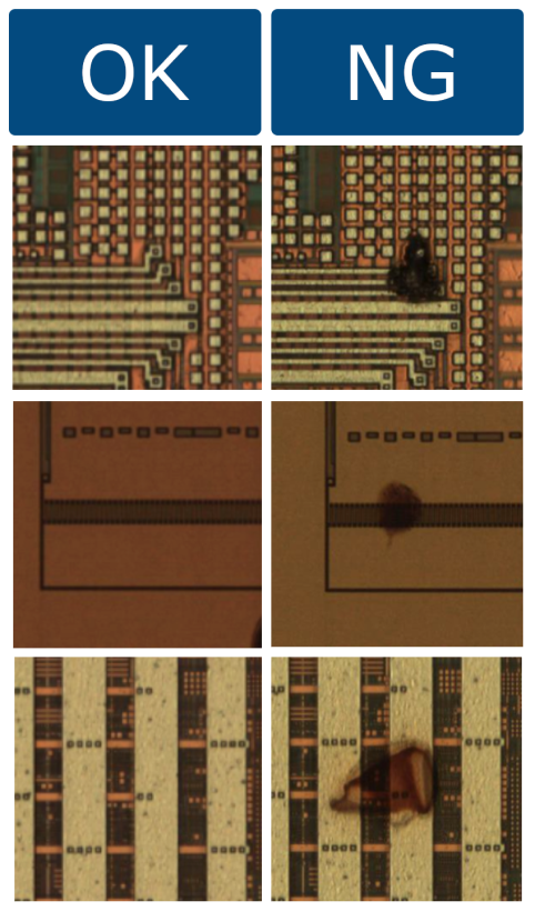
Automatic Defect Detection (ADC)
Inline ADC
Minimize material waste through improved defect detection and quality control processes.
Outgoing ADC
Achieve superior performance with minimal data.
Automated Optical Inspection (AOI)
Minimize material waste through improved defect detection and quality control processes.
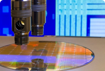
SEM Imaging
Use AI in semiconductor manufacturing to analyze ultra-high-resolution SEM images and detect microscopic defects, such as surface anomalies or particles, that are invisible to the human eye. LandingLens helps improve semiconductor quality control by enabling early defect detection, critical for high-yield production.
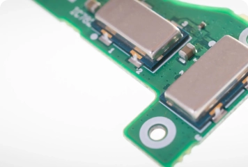
MEMS Inspection
LandingLens supports artificial intelligence in semiconductor manufacturing by inspecting micro-electromechanical systems (MEMS) for surface roughness, cracks, etching errors, and other microscopic issues. These AI-powered inspections enable high-precision analysis of miniature components that traditional systems often miss.
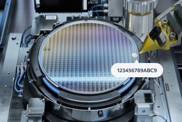
Read Wafer IDs
Streamline traceability across production lines with AI-enhanced OCR technology. LandingLens can read ID numbers on wafers, integrated circuits, and semiconductor components with high accuracy. This capability supports advanced applications of AI in the semiconductor industry, enabling error-free tracking and streamlined process optimization.

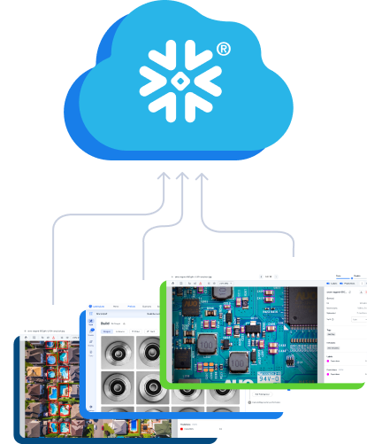
Leverage Your Data in Snowflake
Already have your images in Snowflake? LandingLens is available in the Snowflake Marketplace! This means that LandingLens can directly access the images that you already have stored in Snowflake.
Additionally, you can do it all within the secure, governed boundary of the Data Cloud!