Computer Vision in Semiconductor Device Fabrication

In semiconductor device fabrication, precision is paramount. From microscopic scratches to foreign particles on wafers, every defect detracts from your bottom line.

Empower your wafer and integrated circuit quality control processes with LandingAI. Use LandingLens, our cloud-based computer vision platform, to quickly train and deploy models.

Elevate your standards, boost profitability,
and achieve unparalleled success

by using AI in your semiconductor and integrated circuit production.

Semiconductor Use Cases

See how AI in semiconductor device fabrication can improve quality and efficiency.
The flexible deployment options in LandingLens allow you to seamlessly integrate a LandingLens model into your quality control process.

Automatic Defect Detection (ADC)

Inline ADC
Use a model from LandingLens to catch issues at any stage of the production process. This identifies issues before more value is added to the wafer in downstream tasks, saving you time and money.

Outgoing ADC
A single model in LandingLens can be trained to identify multiple defects for different technologies. Additionally, an automated model can review 100% of your captured images at a highly accurate rate.

Automated Optical Inspection (AOI)
Train a computer vision model that can perform automatic defect classification in an Automated Optical Inspection (AOI) system.

SEM Imaging

SEM Imaging (SEM)

Run computer vision models on images from a scanning electron microscope (SEM), giving you the ability to detect hard-to-see defects.

MEMS Inspection

MEMS Inspection

Detect surface roughness, etching, and cracks in micro-electromechanical systems (MEMS).

Read Wafer IDs

Read Wafer IDs

Combine a LandingLens model with our LandingAI OCR technology to read ID numbers on wafers, semiconductors, and integrated circuits.

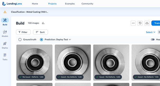
LandingLens Makes Computer Vision Accessible

Create and test your computer vision AI model in minutes. Simply upload a few images, label them, and click “Train”.

Become a Chip Champion with Large Vision Models (LVMs)

Cut Costs. Minimize material waste through improved defect detection and quality control processes.

Save Time. Reduce production cycle times and accelerate time-to-market with efficient manufacturing processes.

Handle Complexity. Your customized LVM can quickly be implemented on multiple different assembly lines.

Achieve Optimal Results. Leverage a data-centric approach to refine process and manufacture higher quality goods.

Leverage Our Know-How. Benefit from our team’s expertise in applying computer vision solutions in real-world scenarios.

Continuously Innovate. Stay ahead of competitors and scale up your manufacturing organization by accessing the latest innovations in computer vision.

Leverage Your Data in Snowflake

Already have your images in Snowflake? LandingLens is available in the Snowflake Marketplace! This means that LandingLens can directly access the images that you already have stored in Snowflake. 

Additionally, you can do it all within the secure, governed boundary of the Data Cloud!

Resources

Blog

Automatic Defect Classification in Wafer Fabrication

Case Studies

Solve Complex Semiconductor Inspection Challenges with Deep Learning

Blog

Introducing Domain-Specific Large Vision Models