


")
Maximizing Yield and Cutting Costs for Semiconductor and MEMS Manufacturers
Semiconductor and MEMS manufacturers around the world are maximizing their yield and reducing expenses through the use of LandingLens. These manufacturers empower advanced technologies and elevate everyday experiences. By implementing automatic defect classification solutions, one of leading manufacturer has achieved a remarkable labor cost reduction of at least 80% wherever these solutions are utilized.
The importance of yield in the semiconductor industry cannot be overstated. It determines the number of usable chips that can be obtained from a single wafer. A high yield translates to greater profitability for manufacturers, while a low yield results in wasted resources and loss of money. As chips become more advanced and production volumes increase, yield becomes even more crucial. Even a slight improvement in yield can have a significant impact on profitability. That’s why semiconductor manufacturers invest heavily in cutting-edge wafer fabrication techniques, process control, and defect detection to enhance their yield.
In this article, we explore how LandingLens, the cloud-based computer vision platform from Landing AI, can optimize your fabrication process, saving you time and money.
Challenges with Manual Inspections
Chip makers often use many machines across each fab to capture images of anomalies on wafers throughout the many stages of the fabrication process. However, these machines cannot accurately classify the anomalies into the correct defect categories. This defect information is crucial for yield enhancement teams to improve production yield and sometimes determine whether a chip should be discarded due to critical defects.
To obtain this valuable information, manufacturers rely on a manual process where a team of inspectors in each fab reviews the images. Unfortunately, this process is slow, expensive, and prone to accuracy issues. It requires a team of twelve inspectors working in shifts around the clock to handle the volume of images from a single fab.
The manufacturer was searching for an automated solution to this problem, but had yet to find a technology that met their precision requirements until they found LandingLens
The LandingLens Solution
Landing AI has partnered with semiconductor manufacturers. By leveraging existing datasets, Landing AI’s solution, LandingLens, helps manufacturers maximize their efficiency and produce high-impact models.
With LandingLens, the workflow is streamlined. Manufacturers start by uploading datasets to projects and take advantage of the platform’s user-friendly labeling tools to clean and label the data efficiently. Training the models is as simple as clicking a button. To ensure accuracy, the models are evaluated against a test dataset using the platform’s error analysis tools. Once the models meet the desired specifications, they are ready for deployment.
The initial solution yielded impressive production results in less than a month. Subsequent models were built and deployed even faster. In fact, it’s now possible to train and deploy models in just a matter of hours.
The model training process is not only fast but also produces high-performing models. In addition, LandingLens’ cloud inference service seamlessly integrates into their internal systems. Once a model is deployed, images are automatically queued from their on-premise database and sent to the cloud where a prediction is made and written back to the database. These predictions are used for process control or for making decisions on whether to scrap or not. As a result, a large number of wafer images can now be classified in minutes with increased precision compared to hours.
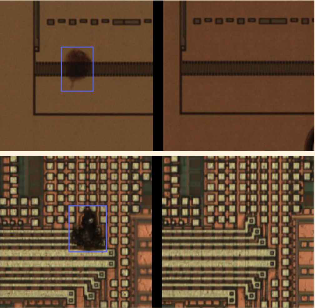


 Sample images (a defective chip on the left vs. a good chip on the right) from automatic defect classification (ADC) solution in optical microscope images Image Source from NXP
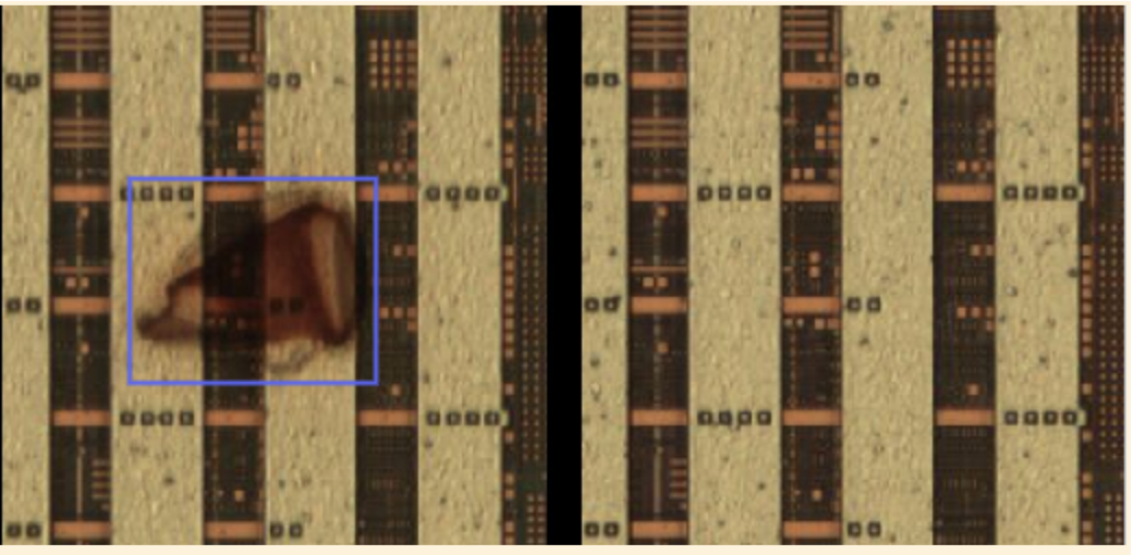
Remarkable Outcomes
Lendinglens has greatly enhanced the classification of defects in semiconductor manufacturing, resulting in several significant advantages:
Precision – Production-grade system aims for a precision of 80%, which is the industry standard. In one deployment case, the LandingLens models demonstrate their ability to not just meet but greatly surpass the requirement with a precision of over 95%. This is a notable enhancement compared to the current standard precision of approximately 70% among existing inspectors.
High Accuracy on Scrap Decisions – Reducing costs in the fabrication process is crucial, especially when it comes to scrapping chips. It is essential to accurately identify and scrap only the faulty chips. The LandignLens models have been extensively tested against subject matter expert labels and have consistently achieved a remarkable accuracy rate of over 99%.
Labor Reduction – LandingLens ADC solutions have consistently proven to reduce manual labeling labor by up to 80%.
Easy Integration – Chip makers have transformed their production process, greatly simplifying the creation and implementation of comprehensive solutions. Instead of waiting for months, they now deliver fully integrated solutions in just a few days.
Generalizable – The projects achieved great success by demonstrating the models’ ability to generalize effectively. In any inspection station, numerous varieties of chips (technologies) are encountered, each with its unique visual characteristics. What sets LandingLens models apart is their proven ability to work well across all these technologies, which is a significant breakthrough. In contrast, previous solutions in this field required programming for each individual technology, making it impractical for many manufacturers, which produces hundreds of technologies in any fab.
One manufacturer can save hundreds of thousands of dollars per facility each year by improving labor efficiency. But that’s not the only benefit. This improvement also leads to process enhancements and increased customer satisfaction.
Future Expansion
The LandingLens solutions have proven to be highly effective for the top semiconductor manufacturers in the industry. They are driving the future growth and expansion of multiple production facilities.
Learn More
Begin your journey with LandingLens computer vision platform for free, or reach out to our team for any guidance!
")